WirelessBR
|

|
WirelessBr
é um site brasileiro, independente, sem vínculos com empresas
ou organizações, sem finalidade comercial, feito por
voluntários, para divulgação de tecnologia em telecomunicações |
|
Integrated Systems Design |
|
Autor:
Leandro Soares Indrusiak (*) |
Esta página
possui figuras grandes. Aguarde a carga se a conexão estiver lenta.
1.
Introduction
Traditionally,
the Electronic Design Automation (EDA) field can be divided in two branches:
integrated circuit design and printed circuit board design. The first branch,
also called VLSI design, covers the design of electronic circuits integrated in
a single chip, while the second branch involves the design of circuit boards,
used to connect together the various parts - mainly integrated circuits - of an
electronic product. The scope of our work is the first forementioned branch, so
when the text refers to the EDA field, we mean the integrated circuits design
activity and its practitioners.
In
this chapter, we will address the evolution of the concept of Integrated Systems,
as well as the design methodologies used to cope with such evolution. Examples
of design automation tools and frameworks are also presented, and their role in the design process is discussed.
2.
Integrated Systems: a definition
In
order to understand the EDA process, we should first take a closer look on the
target of such activity.
Integrated
systems can be described as a heterogeneous composite of programmable modules,
packaged together in a single device. Those modules can be, for instance,
digital or analog circuitry, micromechanical parts, radio frequency (RF),
electro-optical and even electro-biological structures. As important as the
modules themselves, the programming information for each module is also a
product of the design process.
Figure
1, published by the Semiconductor Industry Association, shows the technologies
which are being integrated to the standard CMOS fabrication process, allowing
the production of chips where different types of modules can be put together in
a single die - the so-called System-on-a-Chip (SoC).
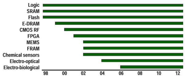
Figure
1: Technologies integrated on SoC in the standard CMOS process [SIA99]
A
long way had to be covered to reach the state where different types of modules
can be put together in a single die. This section analyzes the balance between
the fabrication possibilities and the design capability, which leads to a full
overview on the evolution of the design methodologies in the past 30 years.
Initially,
the fabrication process allowed the creation of digital circuits in a small
scale of integration. To make a better picture, the first microprocessors had
less than 4000 transistors, while currently we are going through
hundreds of million transistors in a die and looking forward to develop
one-billion-transistor chips within the next years. So it is easy to understand
that, in those early days, the focus of the research in the microelectronics
field was on making the fabrication process better, intending to allow higher
density of circuitry per chip. Restricted by such constraint, the complexity of
the integrated circuits design was relatively low, accomplished by small teams
using extremely simple design-aid tools mainly for physical layout edition. But
nowadays, when it is possible to fabricate chips with hundreds of millions of
transistors and to count on a marked demand for products with greater complexity
every year, the design process has turned to be the bottleneck.
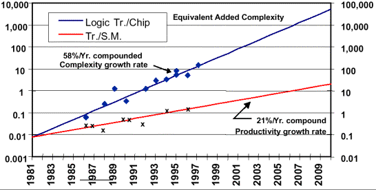
Figure
2: The "Design Gap" [SIA99]
The
"Design Gap" is how it is being called the increasing difference
between the growth of the productivity of design engineers and the growth of the
logic density allowed by the chip fabrication process. Figure shows a graph with
actual numbers and estimations for the years to come.
So
as the need for productivity was getting more and more important, the
development of efficient design methodologies had been the target of many
research groups all over the world. This battle for productivity - which will
probably never end - is discussed in the next session.
3.
Integrated System Design
The
process of the design of integrated systems comprehends the creation and
transformation of different kinds of descriptions, using several domains and
abstraction levels. To cope with the increasing productivity requirements, more
levels, domains and transformations are added to the process.
A
design methodology can be understood as the systematic use of a set of
transformations, from the initial description to the final system. Some of the
transformations add new information to the system description, while others are
aimed to verify the correctness of the description or extract from it
information which weren't explicitly there. The former type is usually called
synthesis while the latter, analysis.
In
Figure 3, a typical design flow is depicted, showing the transformations between
different kinds of descriptions.
3.1 Functional Specification and Validation
The
design usually starts in a very high level of abstraction, by describing the
intended functionality of the system: - system-level specification [SAN00]. This
description disregards every implementation detail, focusing only in the system
behavior and its interactions with the external world. The system description
can be done using one or more languages. The SystemC approach [SWA01], for
instance, advocates for a single specification language, in order to ease the
interoperation of design tools and reduce the costs of the design within the
industry. In other hand, the TIMA research group [JER99] and the Ptolomy Project
[LEE01] focus in the interoperation of languages and modeling styles. Other
approaches for system level design include Ocapi [DES00], SpecC [GAJ00], SDL
[ELL97] and Forge [DAV01].
Some
of the languages used for system specification have formal semantics, with
underlying mathematical structure - e.g., Petri nets, finite state machines -
while others derive from previously developed HDLs or programming languages.
Visual languages and/or visual extensions for textual languages are also among
the alternatives for system modeling.
After
the modeling step, a functional validation takes place. This is done by
simulating or executing the system model, so that the functionality can be
verified. No performance tests are executed on this phase, because no
assumptions about the implementation were made yet. If the functional
requirements of the system are not met, the model should be reviewed, otherwise
the next step of the design flow - model partitioning - is started.
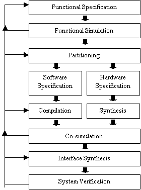
Figure
3: Simplified System Design Flow
3.2
Partitioning
The
partitioning problem can be defined as the mapping of the expected system
functionality to the components which are expected to build the system. Examples
of components in typical hardware/software systems are standard processors or
microcontrollers - and the software to be executed on them -, custom ASIC chips,
memories, busses, configurable logic. So, the partitioning procedure takes as
input a functional model of the system and separates the functions which are
going to be implemented by each one of the components. It is important to notice
that the procedure actually starts by the decision on which components will
actually be part of the implemented system. This decision, obviously, strongly
influences the partition itself.
The
concept of platform-based design [SAN00] was introduced in order to reduce the
complexity of this task. According to this concept, the set of components which
is used to build a system is strongly related to its application domain. So, by
establishing a well defined set of components - a platform - and by validating
it in a particular application type, it could be reused in future designs within
such domain. By relying on already developed and validated platforms, the
partitioning step can be done more easily, by mapping automatically the system
functionality to the platform modules. Companies such as Coware [VAN00] and
Cadence [CAD01] are known to support the concept of platforms.
Besides
the choice of the system components to which the functionality will be mapped,
other key issues on the partitioning step must be highlighted: abstraction level
of the functional specification (task level, behavioral level, etc.),
granularity (amount and complexity of the functional units resulted by the
decomposition of the functional specification) and the details about the
partitioning algorithm itself (metrics of quality, cost function, solution space
covering strategy, etc.) [BEC97].
3.3
Software and Hardware Specification, Simulation and Implementation
Usually,
a great amount of the system functionality is mapped into software during the
partitioning step. [ARN00] states that up to 80% of a system is software running
on a platform of general purpose or custom processors (CPU and/or DSP) tightly
coupled with unique dedicated hardware. While the software part show more
flexibility, allowing simpler error correction and upgrades, the part
implemented in dedicated hardware has superior performance, so it is used for
the time-critical functionality of the system.
The
software specification generated from the partitioned system description is
usually programming language source code. When the platform where the software
is going to run is pre-existent, there is usually available a compiler to
generate object code, as well as a set of software drivers, so the software
modules can access the dedicated hardware parts transparently. In most cases, a
simulation engine is also available, so the software modules can be tested over
a software emulation of the hardware platform. Minor corrections may be done
directly in the generated source code, but major revisions should be done in the
system model, so the partitioning can be re-done to ensure better results.
However,
in most of the cases there is some customization in the underlying platform.
This customization is defined by the hardware specification taken from the
partitioned system description. It is usually HDL code, which should be
simulated together with the software modules and its underlying platform. This
procedure is called co-simulation. Again, minor corrections can be done directly
in the HDL code, but if major corrections are necessary, it should be done in
the system specification. Once the co-simulation shows the desired results, the
synthesis of the hardware modules can start, as well as the synthesis of the
communication structure that allows the interoperation of the hardware modules
and the platform that runs the software part. Such synthesis is by itself very
complex and will be described in details in subsection 3.3.1. Once the
customization of the underlying platform is done, it is necessary to ensure that
the software modules would be able to run optimally over it. New drivers must be
implemented, to make the bridge between the software modules and the customized
hardware, and - if the software processing hardware was also customized - new
compilers must be generated.
3.3.1
Hardware Synthesis
The
synthesis of the hardware modules and the communication circuitry is a very
complex task by itself. After the system partition and communication generation,
those modules are described in a high level of abstraction using a HDL. In order
to translate such abstract description into actual hardware, a set of model
transformations must be done. Such process, depicted in Figure 4, is based on
techniques developed over more than three decades of research.


Figure
4: Hardware Synthesis
In
the behavioral synthesis, the high level model of the hardware part decomposed
in a three sub-models:
·
a sequence
graph, which defines the operations that must be performed by the circuitry, as
well as the order that the operations should be executed;
·
a set of
functional resources - usually a library of functional blocks - which are
available for the implementation of the
circuitry;
·
set of design
constraints, which specify limits - for size, performance, power consumption,
etc. - that should be respected by the final implementation.
The
behavioral synthesis comprehends three stages. In the first stage, each
operation on the sequence graph is scheduled, respecting the dependencies among
them. Once the schedule is done, each operation must be assigned to a functional
block. To minimize area, each functional block must perform several
non-concurrent operations. So, in the second stage the resource sharing is
optimized so that a minimum number of functional blocks can be found, still
respecting the schedule previously done. Finally, the third stage - resource
allocation - can be done, by explicitly assigning each operation to a functional
block.
Following
the synthesis flow, the next transformation - called logic synthesis - has as
main goal the generation of a logic description of the circuit. The logic
description - a net of logic gates, which are modeled as a set of boolean
equations - is necessary for the physical synthesis later on. Furthermore,
several techniques can be applied during the logic synthesis in order to reduce
the complexity of the final circuit, by reducing area and power consumption or
even easing the testability.
Finally,
the physical synthesis has the responsibility on the generation of the physical
layout of the circuit. Usually, this is done by mapping each logic block -
resulting from the logic synthesis - into pre-defined layout cells. Such cells
are usually grouped in a library, possibly with alternatives for each cell -
tailored for smaller area, higher performance, lower power consumption, etc. The
libraries are closely related to the circuit fabrication process, so after this
stage should probably not possible to change the circuit fabrication technology.
After
the technology mapping, the relative position of the layout cells is then
defined, and the layout of the connections among them - and the external world -
are generated, following the connection between the blocks in the logic netlist
in a procedure called Place&Route. Very complex algorithms are used in this
stage, in order to minimize the number and the length of the connections,
because such factors affect significantly the circuit performance. Once the
cells are placed and routed, the circuit is ready to go for fabrication.
4.
References
[ARN00]
ARNOUT, G. C for System Level Design. http://www.systemc.org/papers/coWare.pdf
[BEC97]
BECKER, J. A Partitioning Compiler for Computers with Xputer-based
Accelerators. Doctoral Thesis. Fachbereich Informatik der Universität
Kaiserslautern, 1997.
[CAD 01]
CADENCE DESIGN SYSTEMS, INC. Datasheet: Cadence Virtual Component
Co-Design. http://www.cadence.com/datasheets/vcc_environment.html
[DAV01]
DAVIS, D. et. al. Forge-J: High Performance Hardware from Java. http://www.xilinx.com/forge/forge.htm
[DES00]
DESICS Division. "Ocapi-xl". http://www.imec.br/ocapi
[ELL97]
ELLSBERGER, J.; HOGREFE, D.; SARMA, A. SDL - Formal Object-Oriented
Language for Communication Systems, Prentice Hall, 1997, 312 p.
[GAJ00]
GAJSKI, D. et al. The SpecC Methodology. http://www.ics.uci.edu/~specc
[JER99]
JERRAYA, A.A. et al. Multilanguage Specification for System Design and
Codesign, TIMA RR-02-98/12 ; chapter
in "System-level Synthesis", NATO ASI 1998 edited by A. Jerraya and J.
Mermet, Kluwer Academic Publishers, 1999.
[LEE01]
LEE, E.A. et al. Overview of the Ptolemy Project. Technical Memorandum
UCB/ERL M01/11. Berkeley: UC Berkeley EE, 2001.
[SAN00]
SANGIOVANNI-VICENTELLI, A. et. al. System Level Design: Orthogonalization
of Concerns and Platform-Based Design. IEEE Transactions on Computer-Aided
Design of Circuits and Systems, Vol. 19, No. 12, December 2000.
[SIA 99]
SEMICONDUCTOR INDUSTRY ASSOCIATION. International Technology Roadmap for
Semiconductors: 1999 edition. Austin, TX:International SEMATECH, 1999.
[SWA01]
SWAN, S. et. al. Functional Specification for SystemC 2.0. http://www.systemc.org
[VAN00]
VANBEKBERGEN, P. CoDesign Strategies For SoC. http://www.coware.com/ppt/ESC2001/sld001.htm
(September 2001)
[ZEC 01]
ZECK, G.; FROMHERZ, P. Noninvasive neuroelectronic interfacing with
synaptically connected snail neurons immobilized on a semiconductor chip. In:
Proceedings of the National Academy of Sciences, v.98, p.10457-1046. Washington:
National Academy of Sciences, 2001.
(*) Leandro Soares Indrusiak
(indrusiak@hop.com.br ) é
professor da PUCRS e sócio da Indrusiak Tecnologia Ltda.
É formado em Engenharia Elétrica pela UFSM, Mestre em Ciência da Computação
pela UFRGS e é aluno do programa de doutorado em Ciência da Computação da
UFRGS.
No corrente ano encontra-se em licença das atividades no Brasil, trabalhando
como pesquisador visitante na Technische Universität Darmstadt, Alemanha.
Atua nas áreas de tecnologia de base (microprocessadores, system-on-a-chip,
projeto de hardware) e de conectividade
(internet, redes wireless ad-hoc, plataforma Java).
Criou a Indrusiak Tecnologia, Ltda. e utiliza sua estrutura para possibilitar
aplicações das novas tecnologias advindas da
pesquisa acadêmica, seja por desenvolvimento próprio ou por parcerias.